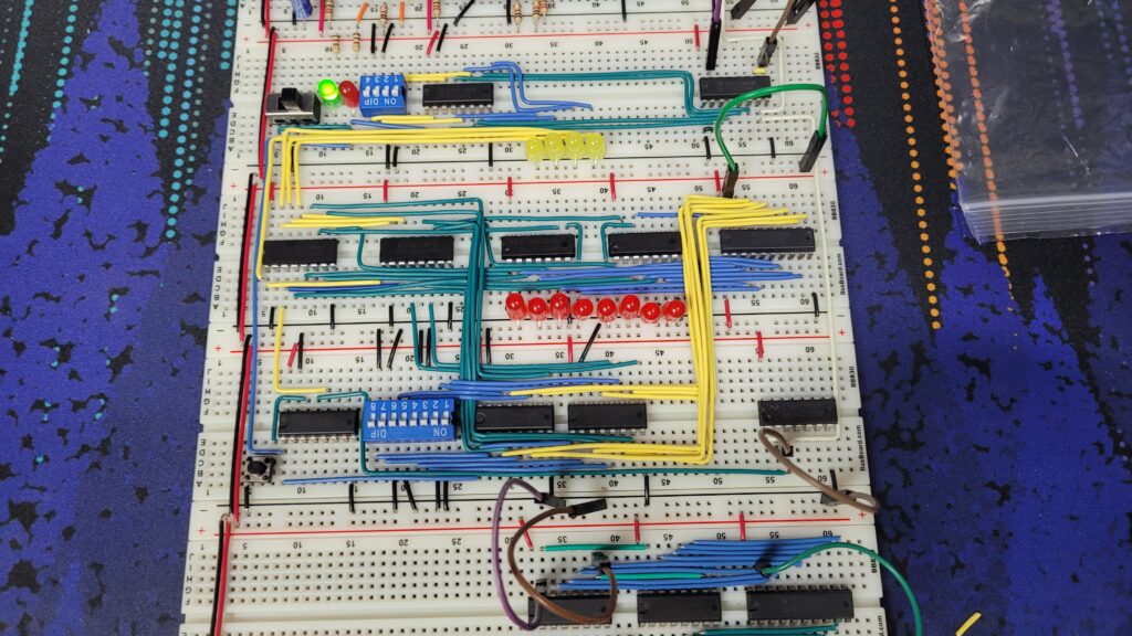
The Random Access Memory guarantees a constant access time for any of its locations. In this case, two 74LS189 RAM modules (each giving 16 words of 4-bit memory) were used to create the 16 bytes of RAM. This is the maximum possible amount of memory possible, since only the lower four bits of the 8-bit architecture are assigned to addresses.
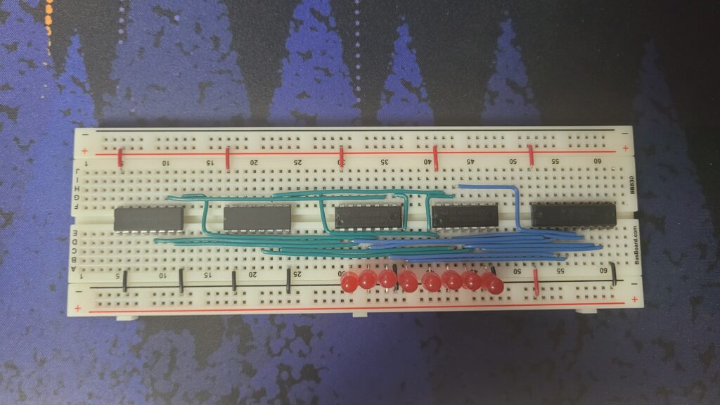
The RAM modules are placed on the left of the breadboard, and two inverters are placed after that, since the RAM modules give an inverted output. Finally, the 74LS245 determines if the RAM values are uploaded to the bus.
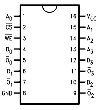
The second pin is the Chip Select, which enables the output of the RAM when low. It is tied to ground so the RAM is always outputting its values. Pins A0 to A3 are the four address lines for each of the 16 words.
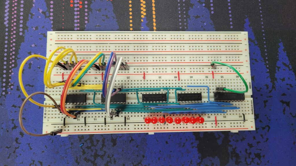
Yellow jumper lines have been temporarily used to set the read/write address and the rainbow colored ones are for loading the 8 bits of data into each word. The brown line toggles the Write Enable.
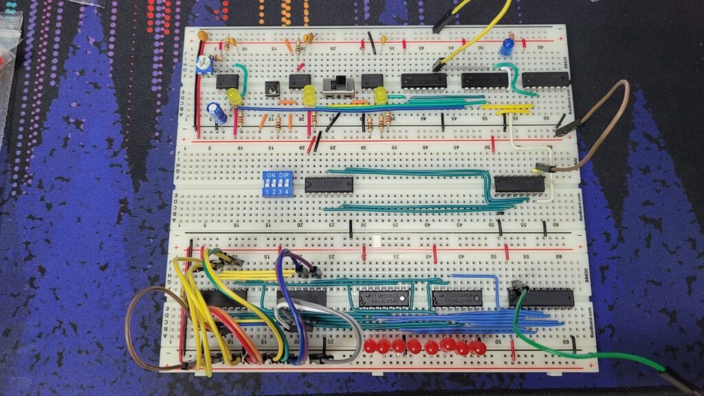
Above the RAM, a DIP switch and 4-bit D register (previously used in the ALU) is added. This combined with some additional logic will allow the user to let the RAM address be determined via bus, or just manually set it with the switches. The 74LS157 Quad 2-to-1 Selector right next to the DIP switch is used to choose the signal to set the address with.
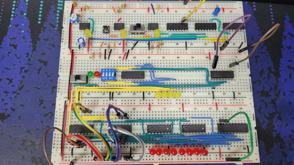
The big switch on the left selects the address mode. The LEDs indicate which mode it is in.
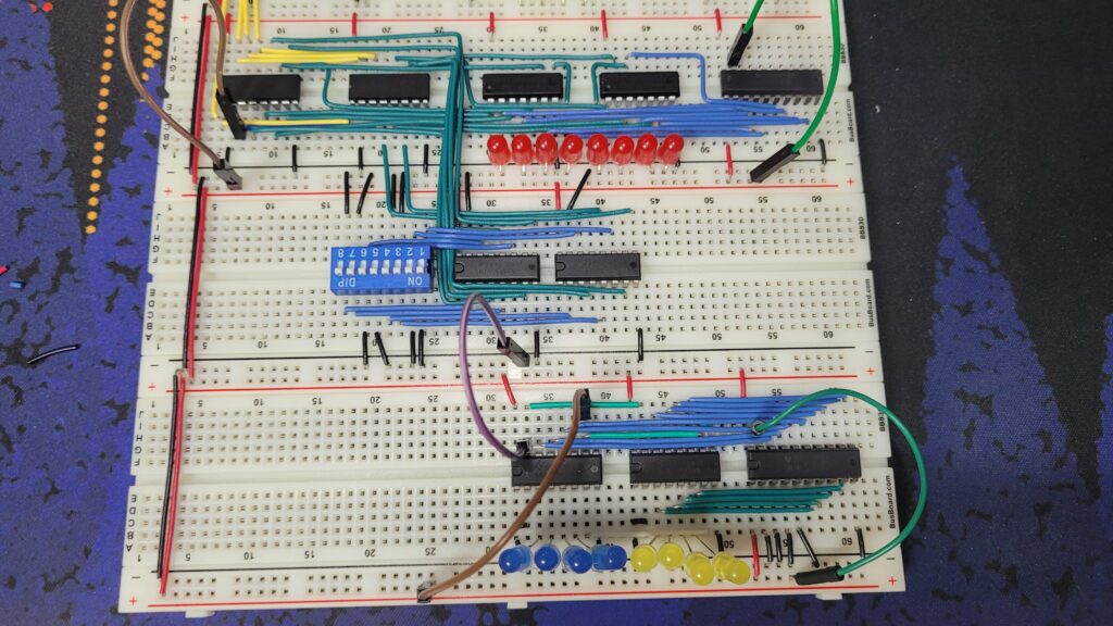
The same procedure is applied to the contents of the RAM, where the DIP switches can be used to manually set the contents of the RAM, which is essentially “programming” it.
Three more selectors are added, one on the left of the DIP switches that will choose if the write values will be from the bus or from the switches.

Finally, a 74LS00 NAND gate is added to the right of the breadboard, where it will combine the clock signal and the write signal to send to the memory modules.
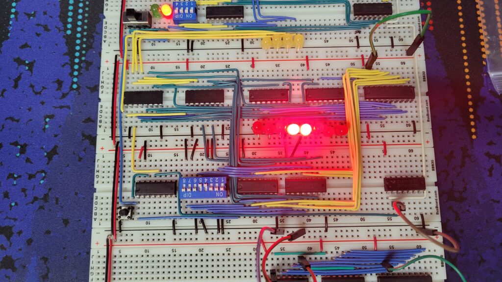
Testing the manual input, selecting manual mode and address 0000 from the top address switches and pushing value 0001 1000 for that address works.
