Registers can temporarily hold data. Most common uses are storing values for calculations. There are general purpose registers for this, and specific registers for instructions, data, addresses too.
4-bit Registers
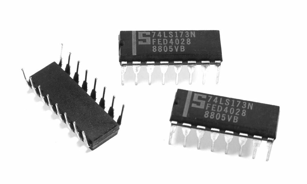
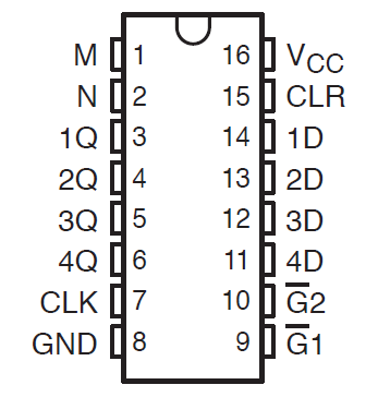
Two 74LS173 4-bit registers can be used to form 8-bit registers. Grounding both M and N pins will activate the outputs on 1Q through 4Q. Grounding both G1 and G2 pins and giving a clock pulse simultaneously will load each bit value into the register through the 1D and 4D pins. In this case the G1 and G2 pins are always enabled, since there will be a control mechanism to decide if the bits will be uploaded to the bus.
Bus interface
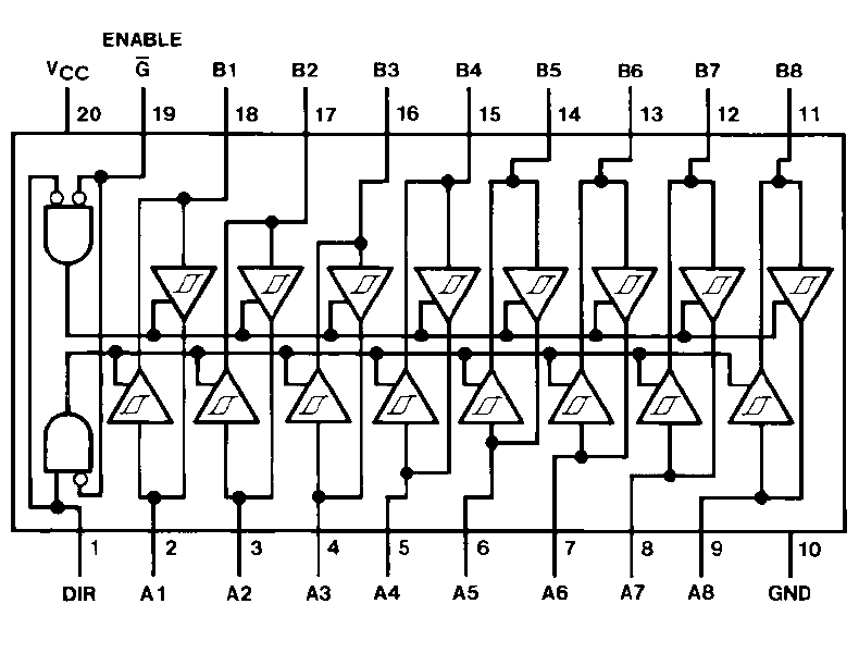
The Octal bus transceiver can be used to determine who gets to use the bus. The DIR line determines which way the signals can go. In this case the DIR pin is always tied to high, which enables data flow from bottom to top. The A line is connected to the bus, and the B line leads to the register inputs. In this configuration, only a clock pulse will be needed to load values into the registers from the bus.
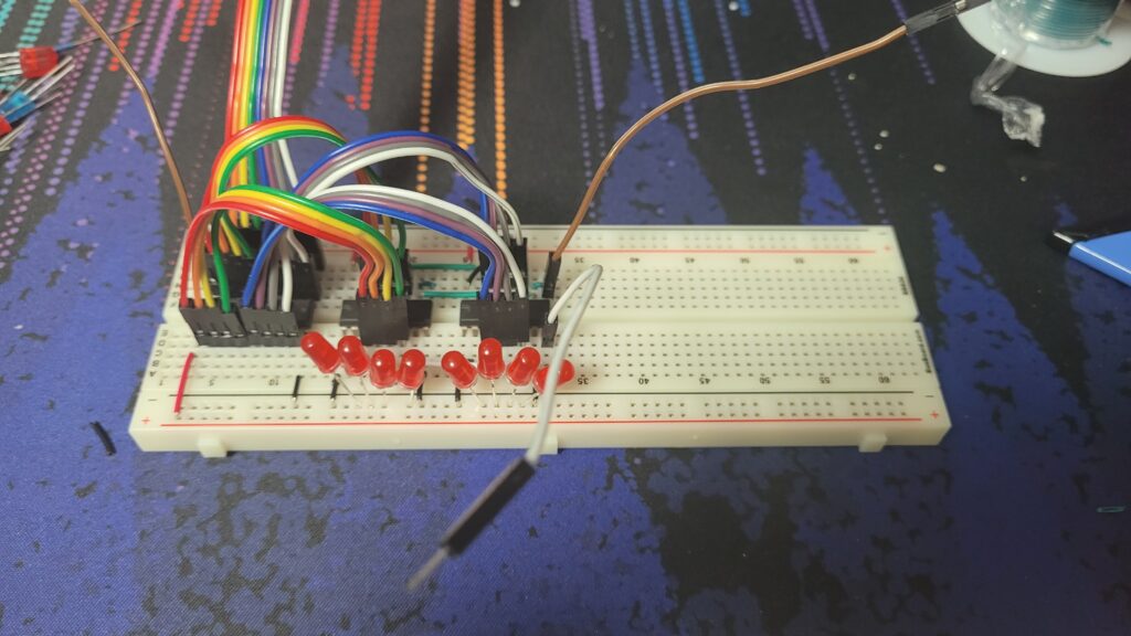
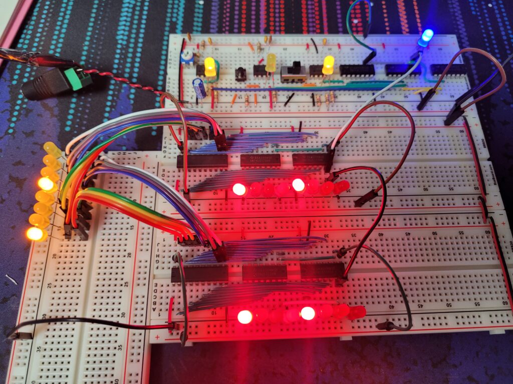
This is a sample register for testing. Beneath all the wires is the bus interface starting from the left, then two 4-bit registers. Register outputs go through the LEDs. The top half of the breadboard is where data from the bus can move in and out.
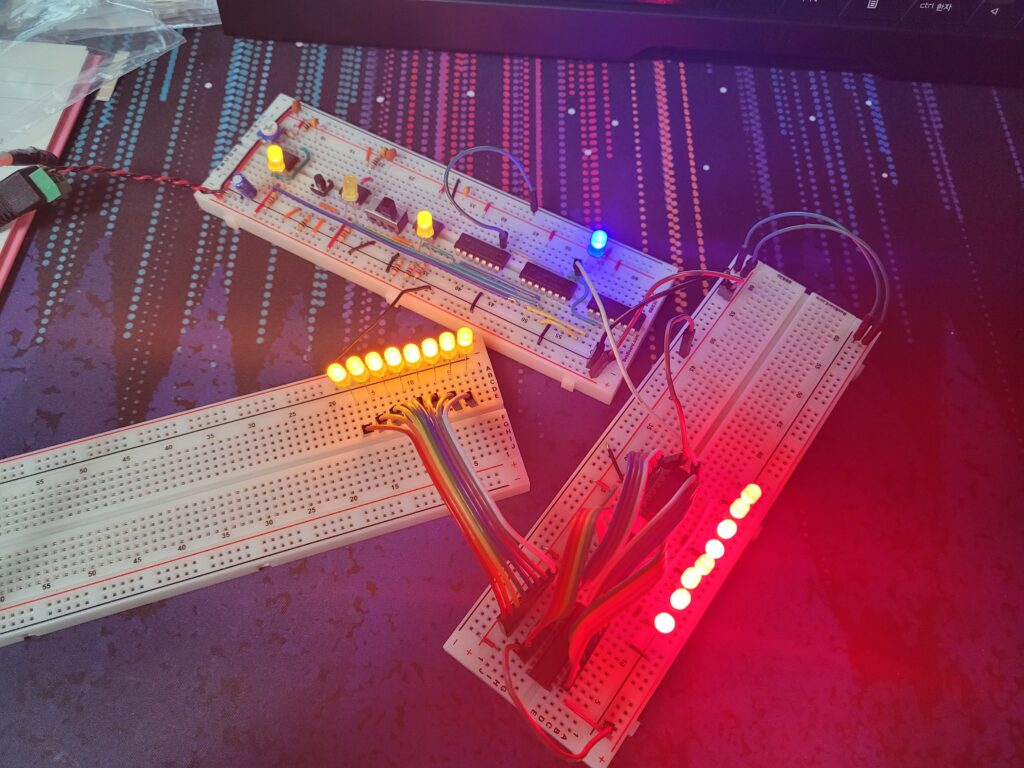
Providing power, the values stored inside the registers are uploaded to the bus (yellow LEDs).
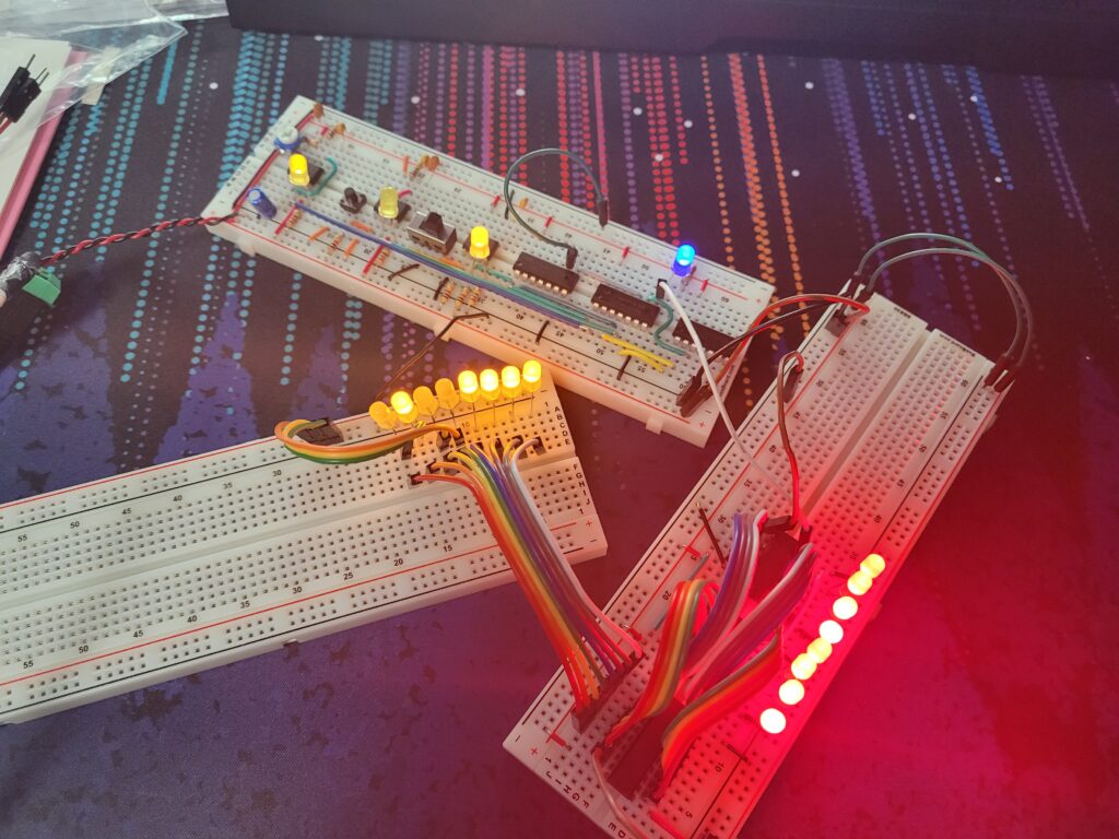
Intentionally grounding a few yellow LEDs at random, a new value of 0100 1111 is created. Enabling the load pin and giving a clock pulse will load the new value in.
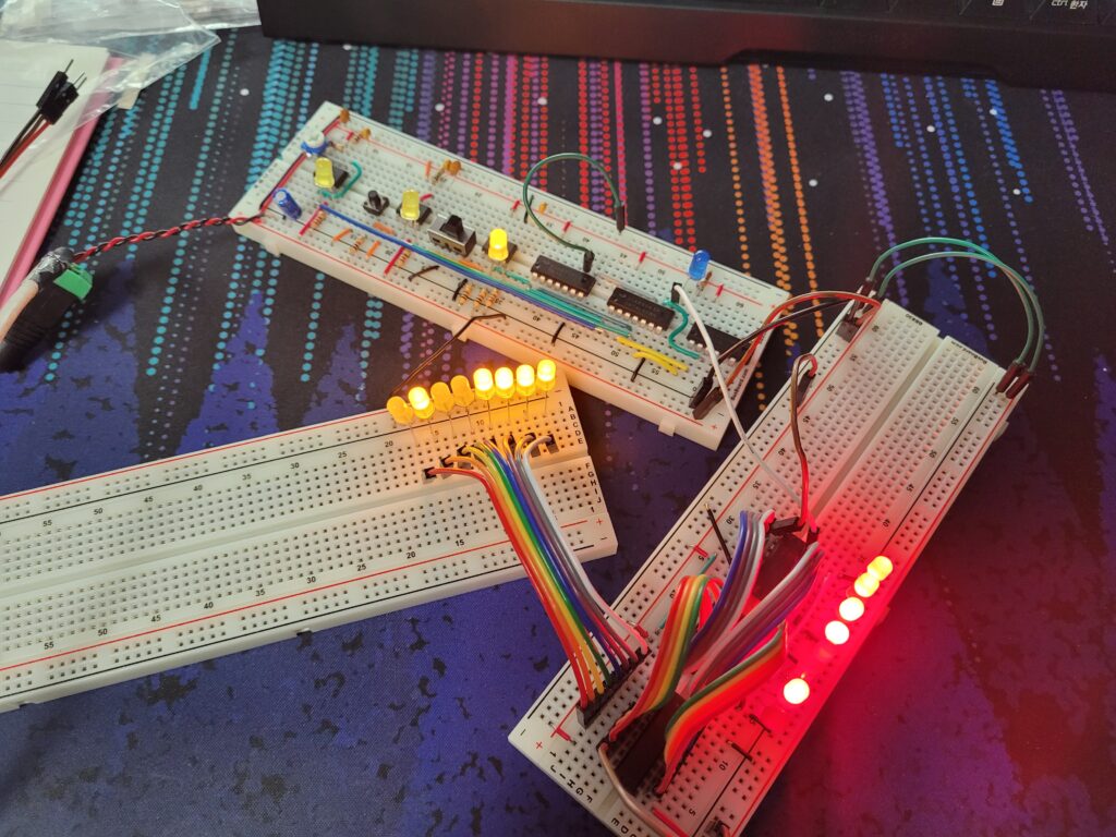
And sure enough, the new value is stored in the registers after a pulse.
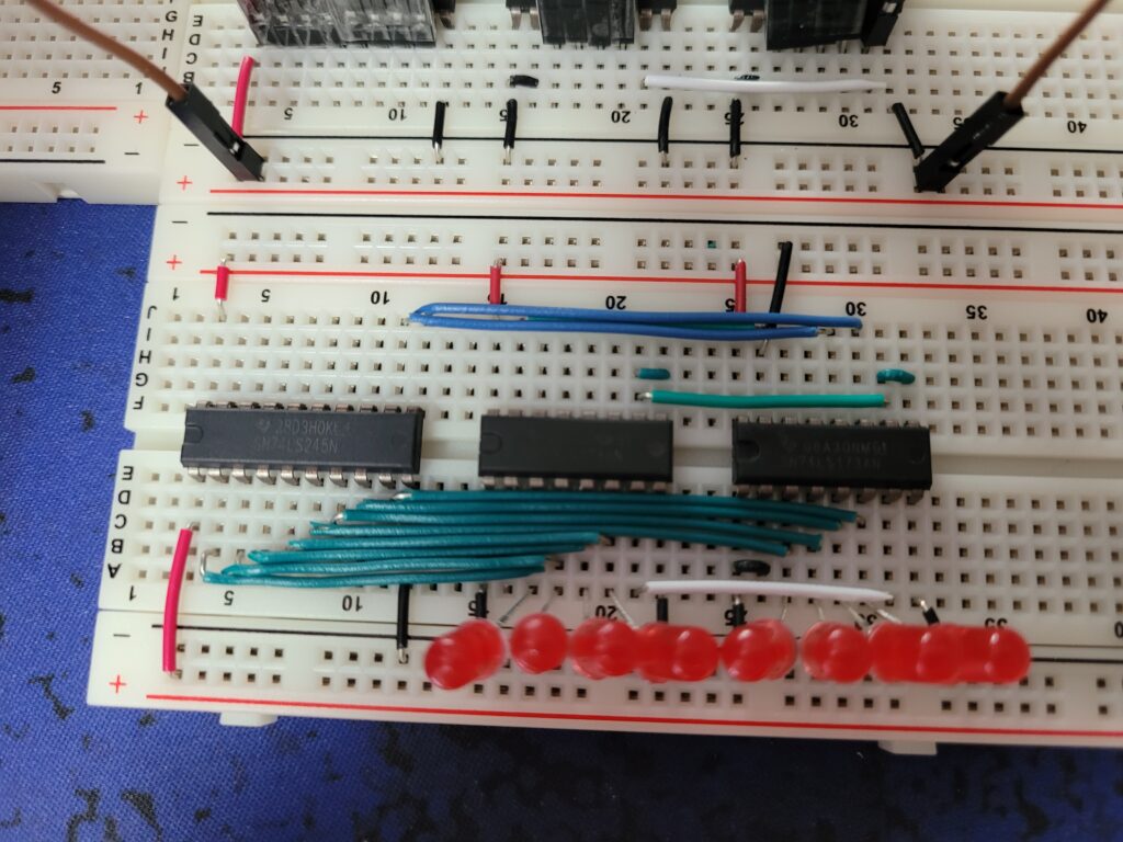
This is the final result after tidying up the wires. The white line is the clock signal which will need to be hooked up to the clock later. Three registers are needed for this CPU, (Register A/B and an Instruction Register), so two more registers are assembled this way.
Moving values between registers
Using two registers and a bus, it is possible to manually copy a value from one register to another.
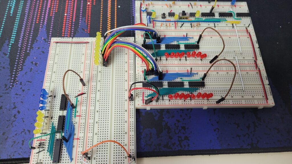
The vertical line of yellow LEDs represent a makeshift bus. The three breadboards on the right is the clock and two registers. The green jumper cables on the registers are for upload enable, and the brown cables are for loading values.
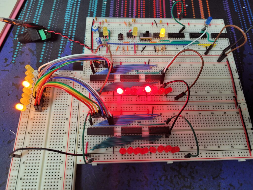
First up is loading a value (1000 1000 in this case) into Register A. This value is also uploaded to the bus.
Register A has upload enabled, and load disabled.
Register B has upload disabled, and load enabled.

Giving a clock pulse in this situation will copy the value from the bus (which was being uploaded by Register A) and store it in Register B, showing the important concept of moving data through a bus.
After this step, it is necessary to go through the steps of finishing the bus usage, by disabling all uploads and loads. Of course this is also performed manually for now.
When the CPU is complete, the user will be able to program it with binary commands. There would need to be another mechanism to read the instruction, and break it down to micro-operations (operations that can be run in one clock pulse). Each micro-operation will automatically handle actions like enabling and disabling upload and load lines.
And after that stage, programming the CPU can be done at a higher level with a homemade assembly language, and will make this process much easier. Which actually coincides with the evolution of computers in real life.
